Saturday, August 18, 2012

Monday, August 13, 2012

Xilinx XC2000 Logic Cell Arrays (LCA) series: XC2064 and XC2018


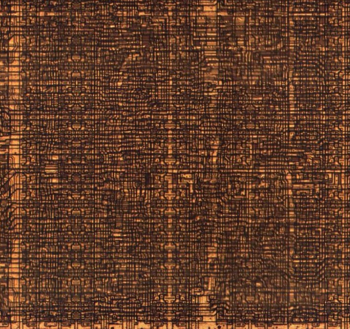
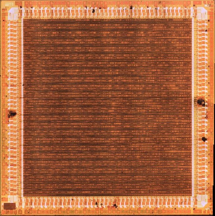
XC2064 w/ 20x objective: http://siliconpr0n.org/map/xilinx/xc2064/top_metal_mit20x/

XC2064 (upper left) w/ 50x objective: http://siliconpr0n.org/map/xilinx/xc2064/top_metal_ns50xu_semipol_ul/

XC2018 w/ 20x objective: http://siliconpr0n.org/map/xilinx/xc2018/top_metal_mit20x/

If you've looked at the latest Xilinx datasheet you will be overwhelmed by a sea of features / acronyms: DCMs, PLLs, multipliers, block RAM, 10s of I/O standards, GTP transceivers, and many more.  Back in my day (alright, to be honest these chips are older than I am) there were just IOBs, CLBs, and interconnect.  Heck, I don't think there was even dedicated clock routing.  The best you had were longer wires.  I don't see any mention of HDL either in the XACT users manual, I think these were schematic driven and sometimes routed by hand.  Finally, I guess the term FPGA hadn't been coined yet so its actually known as a "Logic Cell Array (LCA)" in the datasheet.

A handful of people have expressed interest in the XC2000 series as its the first FPGA.  The first is a XC2064, a 8x8 CLB grid, while the second is its larger brother the XC2018, a 10x10 CLB grid.


Not surprisingly, the cells are nearly the same.  The first is an XC2064 CLB and the second is an XC2018 CLB.


I had been hoping this chip was finally going to answer the question of how the Xilinx internal chip numbers map to package numbering.  Presumably die numbers are decided by engineering and marketing decides the product name later.  The XC2064 roughly matches up and I guess things just diverge from there.


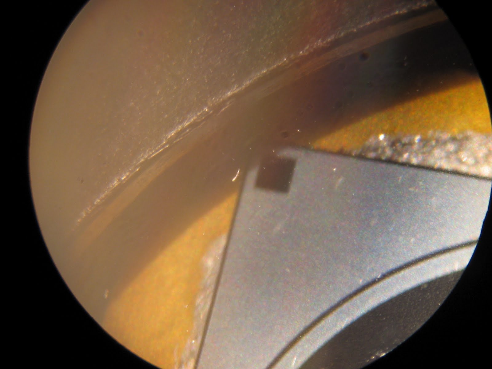
As a process note, the XC2064 had its bond wires "plucked" by about 1 minute in sonicated 10 mL concentrated HCl : 10 mL H2O, :0.5 mL WFNA.  The XC2018 was in the same solution for 10 seconds as the first gave too much damage.  The power pad (top) had the most severe damage anywhere on the chip where as the pad below is more typical.  I will reduce time and/or concentration even further next time.

As a final plug, looking through the ISE 4 user manual, I couldn't help but notice that ISE doesn't change much except for some sometimes useful feature creep crowding up the display.  Not that I really mind that, but with ISE's stability problems I can finally confirm my suspicions that its legacy code that likely hasn't had a well deserved rewrite in at least 10 years.  I couldn't get the DOS XACT program to run but I sure hope that doesn't look the same at least.  However, the message I got when installation failed seems to still be present in ISE so even if its changed appearance its likely kept the same core.

Sunday, June 17, 2012

Tundra CA20C03A


Map: http://siliconpr0n.org/map/tundra/ca20c03a/
Wiki: http://siliconpr0n.org/archive/doku.php?id=mcmaster:tundra:ca20c03a


Corporate headquarters are (were? bought by ON Semi) in Pocatello, Idaho as indicated by the flower / bullet hole / splat:


What caught my interest was that this is a sea-of-gates IC of which I don't see too many.  Marked up layout example with some (not all) transistors marked:


One of the wires to the upper right of Q4 doesn't appear to have a contact.  Not sure whats the deal with that.

In short, a sea of gates designer only creates metal masks to save money.  They pick from a library of predetermined chip sizes and padframes.  Transistors form by routing to the strips of poly crossing the active areas.  Logic gates are separated by occasional gaps in the active areas (as seen above) as well as tying areas high/low to prevent current from flowing.   There is a lot of non-linear routing.  I'm not sure if this is from using a detailed cell lib or if it had a lot of custom layout.  As a result, there are large areas of unused active / poly areas.

Saturday, June 9, 2012

ST 24C02


Wiki: http://siliconpr0n.org/archive/doku.php?id=mcmaster:st:24c026
Map: http://siliconpr0n.org/map/st/24c02/top_metal__ns50xu/

I want to do a more detailed writeup at some point but here are some quick thoughts.  This 256 byte EEPROM chip was much larger than I was expecting.  Close up of some of the cells:


The charge pump can be seen in the lower right hand corner which is identified by the large capacitors:


 At a quick look what may be the output there appear to be a "high voltage" diode string:


Another interesting thing is that I'd expect a chip this small to be fully custom due to the volume market it targets.  You can see a fair amount of diagonal routing so presumably that's at least somewhat true.  However. one of the markings of a larger chip are standard cells.  Of course, even in a fully custom chip there are some regular patterns for repeated circuits so I'm really only talking about glue logic.  There are a few rows of what look like standard cells (highlighted in red):


However, notice the one highlighted in green has  slightly different width than the ones below it.  Additionally,the left and right bank don't actually have the same width as the right is a little narrower.  So if they did use standard cells and not so much a standard cell layout methodology they must be from several different sized libraries.

Wednesday, May 23, 2012

Intel 486DX (80486)


Wiki: http://siliconpr0n.org/archive/doku.php?id=mcmaster:intel:80486dx

Map: http://siliconpr0n.org/map/intel/80486dx/mit5x/

The Intel 80486, more commonly known as an i486, added on chip cache and an FPU over the 80386.  The caches are easily visible as the black areas to the left.  I'm not sure which of the random logic areas are the FPU, maybe a comparison with a 386 would make it obvious.  I assumed there was no 80487, but it looks like there is abeit used in a creative upgrade path where you don't need your CPU anymore.

Intel logo:


And designer initials:


Roughly 70 people working on the chip.  It looks like some have 3 initials to clarify duplicates, but it does make me wonder how it was decided how represented the 2 initial versions.  Also unclear of grouping, is not alphabetical by first or last name.

I was also a bit surprised to see the mask ROM at the bottom.  Maybe microcode?  I don't think Intel microcode could be updated until later but would make sense that it was still easier to design with hard coded microcode.

The die shot also looks similar to the 80486DX2 picture on Wikipedia (CC-BY-SA Matt Britt / Matt Gibbs):


While things are in the same general place it looks like there were some layout changes between the two as components are roughly the same size but look to be laid out a little different.  It also could be a difference between epi and inspection scope illumination.

One interesting thing I found from on the Wikipedia page: "Although the 486 became obsolete for personal computer applications by the mid-1990s, Intel had continued production for use in embedded systems. In May 2006 Intel announced that production of the 80486 would stop at the end of September 2007." Things do stick around longer than you intend.

I have a 20x objective scan (this is 5x objective w/ 10x relay lens for 50x total) where you can actually see all the wires, will try to stitch and post.

Sunday, May 6, 2012

Intel 1602A: "2048 BIT ELECTRICALLY PROGRAMMABLE READ ONLY MEMORY"


Map: http://siliconpr0n.org/map/intel/1602a_10x/

Okay, so its really a 1702A, but the datasheet says they are the same die and that's what the die is marked.  With a 1973 die copyright this could be one of the oldest pieces of silicon I have.  Not exactly ightning fast by today's standard, but boasts a "fast programming time" of 2048 bits in 2 minutes ie slightly over 17 bits per seconds or about half a second to burn in each byte.

Saturday, April 28, 2012

Intel 80960CF (i960)


Map: http://siliconpr0n.org/map/intel/80960cf/mit5x/

Wiki page:  http://www.siliconpr0n.org/archive/doku.php?id=mcmaster:intel:80960cf

The i960 was a competitor to Intel's x86 processor line.  I've seen them in a number of embedded applications like printers so I guess they had some success.  According to Wikipedia they were phased out in favor of StrongARM.

This specimen is from somewhere in the middle of the lineage.  The die is reasonably large at  11.4 X 15.7 mm (179 mm**2).  Compare to something like the 8051 which has a 3.3 X 3.3 mm die (11 mm).  So, I only scanned this at 5x but you can still see some reasonable detail.  I started a scan at 50x, partially as a stitching challenge, but something shifted about halfway through and went out of focus.  I'll probably still try to stitch the good half and post at some point.  Photographing the whole die at 50x was estimated to take 32 hours and was about 24 hours in when I stopped it.  Even prematurely stopped, this is the largest scan I have ever done and still will yield a 3.5 GP after stitching from about 6200 images.

My thanks to the Lab Rat and friends for the donation.

Sunday, April 22, 2012

Xilinx XC4413


Wiki: http://siliconpr0n.org/archive/doku.php?id=mcmaster:xilinx:xc4413&#map

This is a mask programmed version of the XC4013/E FPGA.  I didn't realize Xilinx had ever made mask programmable FPGAs.  Maybe popular for reducing cost by removing the external flash or increased reliability for aero/mil/medical. 

The datasheet still talks about M2/M1/M0 for configuring the device...not sure how many people would order mask ROM part and then select parallel flash or w/e.  Presumably this input is really either "don't care" or potentially should be set to one of the special "reserved" values.  If the latter was the case it could potentially mean that this is an identical chip to the normal version with an all 0 mask.  Although I have a pile of XC4ks I don't have the exact replacement (XC4013/E) to compare it to.

Sunday, April 15, 2012

Newport 882

Busy this weekend so heres some archival footage. Newport 882 photosensor:


Heres an overview of the inside:

Bonding shot:

Can see some markings in the corner:

Sunday, April 8, 2012

Xilinx XC3090...sort of

This week was going to be a XC3090 which didn't pan out but heres at least something interesting as to why. First, the package was somewhat unusual in that its plastic and ceramic:


The F16600 block in the metal is glued or glass sealed on, not exactly sure which it was. In any case I carefully used a small butane torch and took it off with some pliers. Presumably as I was removing it a particle fell on the die. No big deal, I could just wash it off. I noticed a strange shine but didn't think too much of it at the time, dismissing it as a thick overglass or something. I washed it for a bid and the particle didn't come off. Finally I got a little more aggressive and took some lens tissue to it and it STILL wouldn't come off. Confused I put it under the microscope and poked at it. After a bit of poking:


I poked a hole in the gel covering the die. Its only on the die, not on the gold area. It surrounds the bond wires. Heres some grabbed with tweezers:


So other things came up and didn't get a die photo. I cleaned it with some RFNA (soaked fiberglass strip on top) which is probably done by now but didn't get a chance to clean and photograph it.

Sunday, April 1, 2012

AD534: "Internally Trimmed Precision IC Multiplier"

Map: http://siliconpr0n.org/map/ad/ad534/mit20x__semipol/

Compare with the datasheet mask:

Old map: http://siliconpr0n.org/map/ad/ad534/unitron/ Its not quite a fair comparison though because it also used a point and shoot camera. I forget if that was taken with Unitron or Zeiss (aus Jena) objectives.

Sunday, March 25, 2012

Mostek MK5009P


Map: http://siliconpr0n.org/map/mostek/mk5009p/top_metal_mit20x_semipol/


"Mostek industrial products: Counter Time-Base Circuit". Found this in a junk drawer already opened. It was stored in a vial but it seems to have taken some damage. I meant to rotate the map, might re-upload a fixed version later.

Sunday, March 18, 2012

National Semiconductor DM7474J


"Dual D-Type Positive-Edge -Triggered Flip-Flops With Preset And Clear"

This was decapped by heating with a mini butane torch and dripping water on top so that the glass seal cracked. The lid was then removed and photographed in package. I had some pictures of the pinout and now I'm quite annoyed that the seem to have disappeared.

Saturday, March 10, 2012

AWS scale controller


AWS scales are decent bang for buck. Unfortunately, they don't have reverse voltage protection and mine died after I plugged the wrong polarity adapter into it. Heres to its memory.

Wiki page / map link: http://siliconpr0n.org/archive/doku.php?id=mcmaster:aws:scale1

Still on board:


This chip uses aluminum bond wires which are less common but maybe more so for high volume electronics. I don't know exactly how many of these they sell but anything that is COB tends to fall under that category. I used H2SO4 to decap it and so while the PCB has been de-epoxied the copper traces are still intact.

Another interesting thing is that it has bus cheesing (the slits in the power rails around the chip) as well as fill patterns which generally suggests 350 nm or less and/or CMP. However, it appears to be non-planarized as you can see wires making imprints as they cross.

Sunday, March 4, 2012

Xilinx XC9536XL


Wiki page / map link

Apologies but this ones a bit filthy. I've gotten better at cleaning things but took this a while ago.

The datasheet describes this as being two "54V18 Function blocks" meaning two areas with 54 inputs and 18 outputs. The die is pretty symmetric so its easy to guess where these top level blocks are.