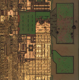
XC2064 w/ 20x objective:
http://siliconpr0n.org/map/xilinx/xc2064/top_metal_mit20x/
XC2064 (upper left) w/ 50x objective:
http://siliconpr0n.org/map/xilinx/xc2064/top_metal_ns50xu_semipol_ul/
XC2018 w/ 20x objective:
http://siliconpr0n.org/map/xilinx/xc2018/top_metal_mit20x/
If you've looked at the latest Xilinx datasheet you will be overwhelmed by a sea of features / acronyms: DCMs, PLLs, multipliers, block RAM, 10s of I/O standards, GTP transceivers, and many more. Back in my day (alright, to be honest these chips are older than I am) there were just IOBs, CLBs, and interconnect. Heck, I don't think there was even dedicated clock routing. The best you had were longer wires. I don't see any mention of HDL either in the XACT users manual, I think these were schematic driven and sometimes routed by hand. Finally, I guess the term FPGA hadn't been coined yet so its actually known as a "Logic Cell Array (LCA)" in the datasheet.
A handful of people have expressed interest in the XC2000 series as its the first FPGA. The first is a XC2064, a 8x8 CLB grid, while the second is its larger brother the XC2018, a 10x10 CLB grid.
Not surprisingly, the cells are nearly the same. The first is an XC2064 CLB and the second is an XC2018 CLB.
I had been hoping this chip was finally going to answer the question of how the Xilinx internal chip numbers map to package numbering. Presumably die numbers are decided by engineering and marketing decides the product name later. The XC2064 roughly matches up and I guess things just diverge from there.
As a process note, the XC2064 had its bond wires "plucked" by about 1 minute in sonicated 10 mL concentrated HCl : 10 mL H2O, :0.5 mL WFNA. The XC2018 was in the same solution for 10 seconds as the first gave too much damage. The power pad (top) had the most severe damage anywhere on the chip where as the pad below is more typical. I will reduce time and/or concentration even further next time.
As a final plug, looking through the ISE 4 user manual, I couldn't help but notice that ISE doesn't change much except for some sometimes useful feature creep crowding up the display. Not that I really mind that, but with ISE's stability problems I can finally confirm my suspicions that its legacy code that likely hasn't had a well deserved rewrite in at least 10 years. I couldn't get the DOS XACT program to run but I sure hope that doesn't look the same at least. However, the message I got when installation failed seems to still be present in ISE so even if its changed appearance its likely kept the same core.


