Wednesday, May 23, 2012

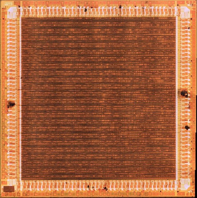
Intel 486DX (80486)


Wiki: http://siliconpr0n.org/archive/doku.php?id=mcmaster:intel:80486dx

Map: http://siliconpr0n.org/map/intel/80486dx/mit5x/

The Intel 80486, more commonly known as an i486, added on chip cache and an FPU over the 80386.  The caches are easily visible as the black areas to the left.  I'm not sure which of the random logic areas are the FPU, maybe a comparison with a 386 would make it obvious.  I assumed there was no 80487, but it looks like there is abeit used in a creative upgrade path where you don't need your CPU anymore.

Intel logo:


And designer initials:


Roughly 70 people working on the chip.  It looks like some have 3 initials to clarify duplicates, but it does make me wonder how it was decided how represented the 2 initial versions.  Also unclear of grouping, is not alphabetical by first or last name.

I was also a bit surprised to see the mask ROM at the bottom.  Maybe microcode?  I don't think Intel microcode could be updated until later but would make sense that it was still easier to design with hard coded microcode.

The die shot also looks similar to the 80486DX2 picture on Wikipedia (CC-BY-SA Matt Britt / Matt Gibbs):


While things are in the same general place it looks like there were some layout changes between the two as components are roughly the same size but look to be laid out a little different.  It also could be a difference between epi and inspection scope illumination.

One interesting thing I found from on the Wikipedia page: "Although the 486 became obsolete for personal computer applications by the mid-1990s, Intel had continued production for use in embedded systems. In May 2006 Intel announced that production of the 80486 would stop at the end of September 2007." Things do stick around longer than you intend.

I have a 20x objective scan (this is 5x objective w/ 10x relay lens for 50x total) where you can actually see all the wires, will try to stitch and post.

Sunday, May 6, 2012

Intel 1602A: "2048 BIT ELECTRICALLY PROGRAMMABLE READ ONLY MEMORY"


Map: http://siliconpr0n.org/map/intel/1602a_10x/

Okay, so its really a 1702A, but the datasheet says they are the same die and that's what the die is marked.  With a 1973 die copyright this could be one of the oldest pieces of silicon I have.  Not exactly ightning fast by today's standard, but boasts a "fast programming time" of 2048 bits in 2 minutes ie slightly over 17 bits per seconds or about half a second to burn in each byte.

Saturday, April 28, 2012

Intel 80960CF (i960)


Map: http://siliconpr0n.org/map/intel/80960cf/mit5x/

Wiki page:  http://www.siliconpr0n.org/archive/doku.php?id=mcmaster:intel:80960cf

The i960 was a competitor to Intel's x86 processor line.  I've seen them in a number of embedded applications like printers so I guess they had some success.  According to Wikipedia they were phased out in favor of StrongARM.

This specimen is from somewhere in the middle of the lineage.  The die is reasonably large at  11.4 X 15.7 mm (179 mm**2).  Compare to something like the 8051 which has a 3.3 X 3.3 mm die (11 mm).  So, I only scanned this at 5x but you can still see some reasonable detail.  I started a scan at 50x, partially as a stitching challenge, but something shifted about halfway through and went out of focus.  I'll probably still try to stitch the good half and post at some point.  Photographing the whole die at 50x was estimated to take 32 hours and was about 24 hours in when I stopped it.  Even prematurely stopped, this is the largest scan I have ever done and still will yield a 3.5 GP after stitching from about 6200 images.

My thanks to the Lab Rat and friends for the donation.

Sunday, April 22, 2012

Xilinx XC4413


Wiki: http://siliconpr0n.org/archive/doku.php?id=mcmaster:xilinx:xc4413&#map

This is a mask programmed version of the XC4013/E FPGA.  I didn't realize Xilinx had ever made mask programmable FPGAs.  Maybe popular for reducing cost by removing the external flash or increased reliability for aero/mil/medical. 

The datasheet still talks about M2/M1/M0 for configuring the device...not sure how many people would order mask ROM part and then select parallel flash or w/e.  Presumably this input is really either "don't care" or potentially should be set to one of the special "reserved" values.  If the latter was the case it could potentially mean that this is an identical chip to the normal version with an all 0 mask.  Although I have a pile of XC4ks I don't have the exact replacement (XC4013/E) to compare it to.

Sunday, April 15, 2012

Newport 882

Busy this weekend so heres some archival footage. Newport 882 photosensor:


Heres an overview of the inside:

Bonding shot:

Can see some markings in the corner:

Sunday, April 8, 2012

Xilinx XC3090...sort of

This week was going to be a XC3090 which didn't pan out but heres at least something interesting as to why. First, the package was somewhat unusual in that its plastic and ceramic:


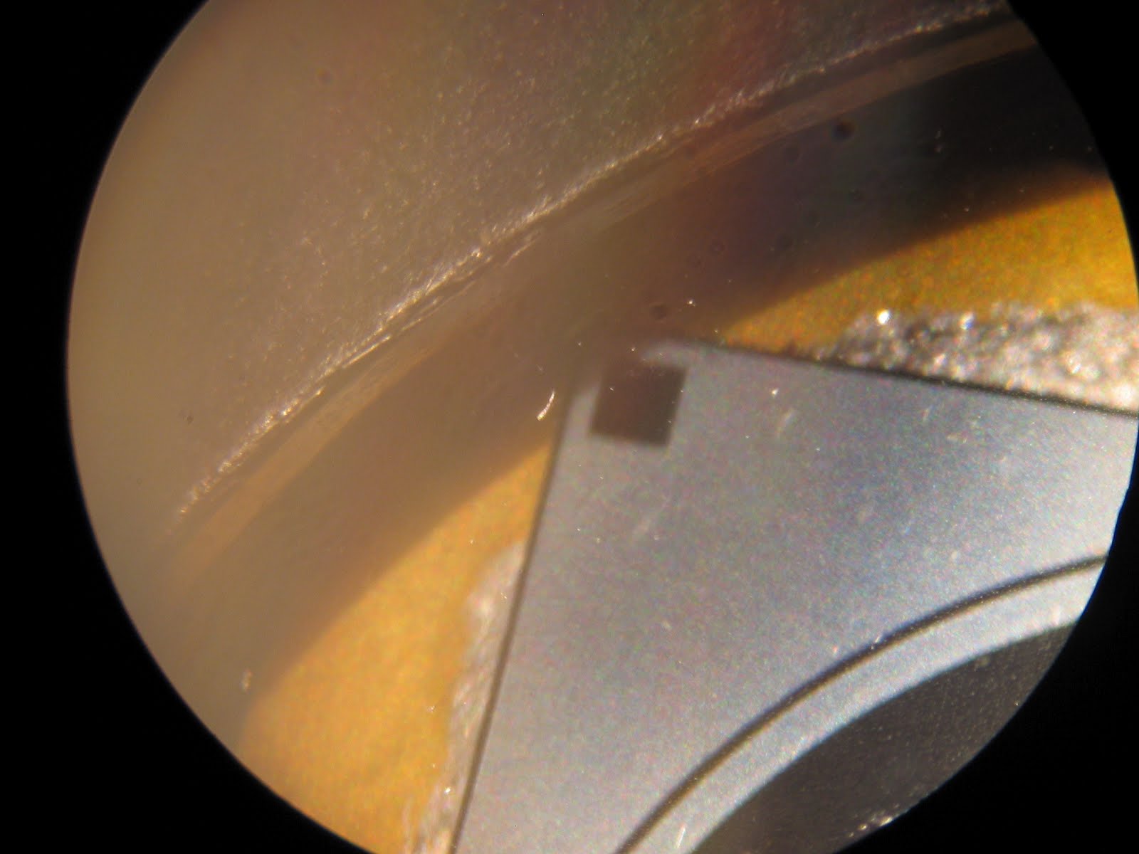
The F16600 block in the metal is glued or glass sealed on, not exactly sure which it was. In any case I carefully used a small butane torch and took it off with some pliers. Presumably as I was removing it a particle fell on the die. No big deal, I could just wash it off. I noticed a strange shine but didn't think too much of it at the time, dismissing it as a thick overglass or something. I washed it for a bid and the particle didn't come off. Finally I got a little more aggressive and took some lens tissue to it and it STILL wouldn't come off. Confused I put it under the microscope and poked at it. After a bit of poking:


I poked a hole in the gel covering the die. Its only on the die, not on the gold area. It surrounds the bond wires. Heres some grabbed with tweezers:


So other things came up and didn't get a die photo. I cleaned it with some RFNA (soaked fiberglass strip on top) which is probably done by now but didn't get a chance to clean and photograph it.

Sunday, April 1, 2012

AD534: "Internally Trimmed Precision IC Multiplier"

Map: http://siliconpr0n.org/map/ad/ad534/mit20x__semipol/

Compare with the datasheet mask:

Old map: http://siliconpr0n.org/map/ad/ad534/unitron/ Its not quite a fair comparison though because it also used a point and shoot camera. I forget if that was taken with Unitron or Zeiss (aus Jena) objectives.