Sunday, December 2, 2012
Yellow plaque
Been a while since posting anything since I've been trying to regain CNC capabilities. Although I did a proof of concept I don't have have a smooth workflow yet. Here's some single shots in the meantime.
http://www.siliconpr0n.org/archive/doku.php?id=mcmaster:amd:8080
http://www.siliconpr0n.org/archive/doku.php?id=mcmaster:intel:2716
http://www.siliconpr0n.org/archive/doku.php?id=mcmaster:unknown:yellow_plaque_left_wafer_2032
http://www.siliconpr0n.org/archive/doku.php?id=mcmaster:unknown:yellow_plaque_right_wafer_smc_3007
Saturday, August 18, 2012
ENC28J60
http://siliconpr0n.org/map/microchip/enc28j60/top_metal_ns50xu/
Not exactly the best stitch but its been lying around for a while and so figured "why not"
Not exactly the best stitch but its been lying around for a while and so figured "why not"
Monday, August 13, 2012
Xilinx XC2000 Logic Cell Arrays (LCA) series: XC2064 and XC2018
XC2064 w/ 20x objective: http://siliconpr0n.org/map/xilinx/xc2064/top_metal_mit20x/
XC2064 (upper left) w/ 50x objective: http://siliconpr0n.org/map/xilinx/xc2064/top_metal_ns50xu_semipol_ul/
XC2018 w/ 20x objective: http://siliconpr0n.org/map/xilinx/xc2018/top_metal_mit20x/
If you've looked at the latest Xilinx datasheet you will be overwhelmed by a sea of features / acronyms: DCMs, PLLs, multipliers, block RAM, 10s of I/O standards, GTP transceivers, and many more. Back in my day (alright, to be honest these chips are older than I am) there were just IOBs, CLBs, and interconnect. Heck, I don't think there was even dedicated clock routing. The best you had were longer wires. I don't see any mention of HDL either in the XACT users manual, I think these were schematic driven and sometimes routed by hand. Finally, I guess the term FPGA hadn't been coined yet so its actually known as a "Logic Cell Array (LCA)" in the datasheet.
A handful of people have expressed interest in the XC2000 series as its the first FPGA. The first is a XC2064, a 8x8 CLB grid, while the second is its larger brother the XC2018, a 10x10 CLB grid.
Not surprisingly, the cells are nearly the same. The first is an XC2064 CLB and the second is an XC2018 CLB.
I had been hoping this chip was finally going to answer the question of how the Xilinx internal chip numbers map to package numbering. Presumably die numbers are decided by engineering and marketing decides the product name later. The XC2064 roughly matches up and I guess things just diverge from there.
As a process note, the XC2064 had its bond wires "plucked" by about 1 minute in sonicated 10 mL concentrated HCl : 10 mL H2O, :0.5 mL WFNA. The XC2018 was in the same solution for 10 seconds as the first gave too much damage. The power pad (top) had the most severe damage anywhere on the chip where as the pad below is more typical. I will reduce time and/or concentration even further next time.
As a final plug, looking through the ISE 4 user manual, I couldn't help but notice that ISE doesn't change much except for some sometimes useful feature creep crowding up the display. Not that I really mind that, but with ISE's stability problems I can finally confirm my suspicions that its legacy code that likely hasn't had a well deserved rewrite in at least 10 years. I couldn't get the DOS XACT program to run but I sure hope that doesn't look the same at least. However, the message I got when installation failed seems to still be present in ISE so even if its changed appearance its likely kept the same core.
Saturday, August 11, 2012
Low res die shots
Most of the dies had their bond wires burned off with aqua regia and some stayed in too long...oops.
http://siliconpr0n.org/archive/doku.php?id=mcmaster:intel:p80c32_l7031442b
http://siliconpr0n.org/archive/doku.php?id=mcmaster:intel:p8051ahp_6095_ab080510017_rev_2.1:start
http://siliconpr0n.org/archive/doku.php?id=mcmaster:amd:am29f040b-120jc
http://siliconpr0n.org/archive/doku.php?id=mcmaster:atmel:648_24c02&#package_alt
http://siliconpr0n.org/archive/doku.php?id=mcmaster:atmel:838_24c04_pc_b&#package
http://siliconpr0n.org/archive/doku.php?id=mcmaster:atmel:at29c010a_70jc_9821
http://siliconpr0n.org/archive/doku.php?id=mcmaster:rca:cd4054be_rca_h_910
http://siliconpr0n.org/archive/doku.php?id=mcmaster:phillips:hef4052bt_706800d
http://siliconpr0n.org/archive/doku.php?id=mcmaster:phillips:hef4077bt_d7130pl_hnn00482
http://siliconpr0n.org/archive/doku.php?id=mcmaster:hp:1ql1-0001_npql1a5067_9732
http://siliconpr0n.org/archive/doku.php?id=mcmaster:microchip:24lc512_ism_06412b0
http://siliconpr0n.org/archive/doku.php?id=mcmaster:st:24c01r6_k209l
http://siliconpr0n.org/archive/doku.php?id=mcmaster:ti:68f483k_e4_tl494in
Tuesday, July 24, 2012
DEC 57-19400-04 (D4-6901-5)
DEC PDP-11 CPU(left half). "The Control Chip (DC335) implements the microword access and sequencing functions of the J-11 chip set." (http://www.cpu-collection.de/?l0=co&l1=DEC&l2=PDP-11)
Map: http://siliconpr0n.org/map/dec/57-19400-04/left/top_metal_mit20x/
Wiki: http://siliconpr0n.org/archive/doku.php?id=mcmaster:dec:57-19400-04
Sunday, June 17, 2012
Tundra CA20C03A
Map: http://siliconpr0n.org/map/tundra/ca20c03a/
Wiki: http://siliconpr0n.org/archive/doku.php?id=mcmaster:tundra:ca20c03a
Corporate headquarters are (were? bought by ON Semi) in Pocatello, Idaho as indicated by the flower / bullet hole / splat:
What caught my interest was that this is a sea-of-gates IC of which I don't see too many. Marked up layout example with some (not all) transistors marked:
One of the wires to the upper right of Q4 doesn't appear to have a contact. Not sure whats the deal with that.
In short, a sea of gates designer only creates metal masks to save money. They pick from a library of predetermined chip sizes and padframes. Transistors form by routing to the strips of poly crossing the active areas. Logic gates are separated by occasional gaps in the active areas (as seen above) as well as tying areas high/low to prevent current from flowing. There is a lot of non-linear routing. I'm not sure if this is from using a detailed cell lib or if it had a lot of custom layout. As a result, there are large areas of unused active / poly areas.
Saturday, June 9, 2012
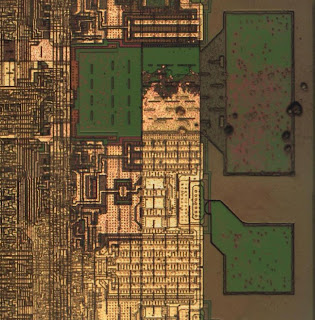
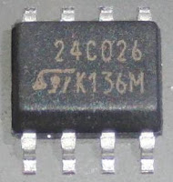
ST 24C02
Wiki: http://siliconpr0n.org/archive/doku.php?id=mcmaster:st:24c026
Map: http://siliconpr0n.org/map/st/24c02/top_metal__ns50xu/
I want to do a more detailed writeup at some point but here are some quick thoughts. This 256 byte EEPROM chip was much larger than I was expecting. Close up of some of the cells:

The charge pump can be seen in the lower right hand corner which is identified by the large capacitors:
At a quick look what may be the output there appear to be a "high voltage" diode string:

Another interesting thing is that I'd expect a chip this small to be fully custom due to the volume market it targets. You can see a fair amount of diagonal routing so presumably that's at least somewhat true. However. one of the markings of a larger chip are standard cells. Of course, even in a fully custom chip there are some regular patterns for repeated circuits so I'm really only talking about glue logic. There are a few rows of what look like standard cells (highlighted in red):
However, notice the one highlighted in green has slightly different width than the ones below it. Additionally,the left and right bank don't actually have the same width as the right is a little narrower. So if they did use standard cells and not so much a standard cell layout methodology they must be from several different sized libraries.
Subscribe to:
Posts (Atom)


