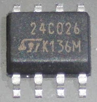
Wiki: http://siliconpr0n.org/archive/doku.php?id=mcmaster:st:24c026
Map: http://siliconpr0n.org/map/st/24c02/top_metal__ns50xu/
I want to do a more detailed writeup at some point but here are some quick thoughts. This 256 byte EEPROM chip was much larger than I was expecting. Close up of some of the cells:

The charge pump can be seen in the lower right hand corner which is identified by the large capacitors:
At a quick look what may be the output there appear to be a "high voltage" diode string:

Another interesting thing is that I'd expect a chip this small to be fully custom due to the volume market it targets. You can see a fair amount of diagonal routing so presumably that's at least somewhat true. However. one of the markings of a larger chip are standard cells. Of course, even in a fully custom chip there are some regular patterns for repeated circuits so I'm really only talking about glue logic. There are a few rows of what look like standard cells (highlighted in red):
However, notice the one highlighted in green has slightly different width than the ones below it. Additionally,the left and right bank don't actually have the same width as the right is a little narrower. So if they did use standard cells and not so much a standard cell layout methodology they must be from several different sized libraries.


No comments:
Post a Comment